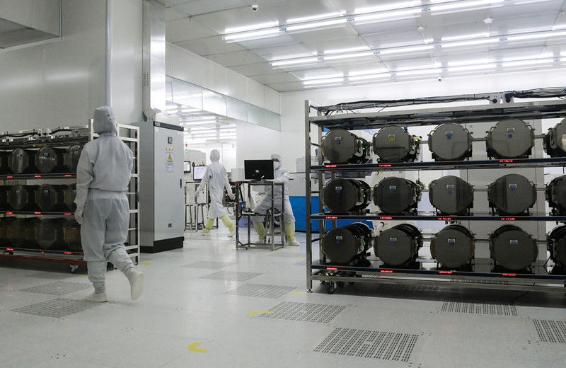
The complete process of chip production generally includes: chip design, chip production, packaging production, cost testing and other major links, among which the chip production process is particularly complicated. The diagram below allows us to understand the process of wafer fabrication together.
1 From sand to wafers
![]()
12 major technological processes from polysilicon to silicon wafer
1) Polysilicon
Polysilicon is a form of elemental silicon. When molten elemental silicon is solidified under supercooled conditions, silicon atoms are arranged in the form of diamond lattices to form many crystal nuclei. If these crystal nuclei grow into crystal grains with different crystal plane orientations, these crystal grains combine to crystallize into polycrystalline silicon. .
2) Crystal growth
3) Monocrystalline silicon ingot
Monocrystalline silicon is a form of elemental silicon. When the molten elemental silicon is solidified, the silicon atoms are arranged in the diamond lattice to form many crystal nuclei. If these crystal nuclei grow into grains with the same crystal plane orientation, these grains combine in parallel to crystallize into single crystal silicon.
4) Crystal trimming and grinding
5) slice
6) Edge rounding
7) Grinding
8) Etching (chemical polishing)
9) Polishing
10) cleaning
11) Check
12) Packaging/Transportation
![]()
2 From silicon wafer to IC
The processing flow from silicon wafer to IC is roughly divided into two steps: front-end and back-end
![]()
2.1 Front-end (FE) process
(1) Wafer preparation
(2) Semiconductor circuit design
(3) Mask preparation
(4) Oxidation stratification
Thermal Oxidation - Creates silicon dioxide, which is the gate of the field effect transistor
(5) Photoresist coating
(6) step exposure
(7) Photolithography
Use ultraviolet light to irradiate the silicon wafer through the mask, and the irradiated area will be easily washed off, and the unirradiated area will remain the same. Then you can engrave the desired pattern on the silicon wafer. Note, At this time, no impurities have been added, and it is still a silicon wafer.
(8) Etching
Etching is divided into dry etching and wet etching:
Dry Etching - Many of the shapes previously etched with lithography are not actually what we need, but are etched for ion implantation. Now we need to use plasma to wash them off, or some structures that do not need to be etched in the first step of photolithography, this step is etched.
Wet etching - further washing off, but using reagents, so it is called wet etching - after the above steps are completed, the field effect tube has been made, but the above steps are generally done more than once, and it is likely to need to be repeated do to meet the requirements.
(9) Ion implantation
Different impurities are added to different positions of the silicon wafer, and different impurities form field effect transistors according to the concentration/position.
(10) Vapor deposition
Chemical vapor deposition (CVD) further refines various substances on the surface. Physical Vapor Deposition (PVD), similar, and can add coating to sensitive parts
(11) Plating treatment
(12) Wafer testing
![]()
2.2 Back-end (BE) process
![]()
• Cures die attach paste to harden and achieve optimum mechanical and electrical properties.
• Products pasted with glue should maintain temperature for a long time (usually around 125~175°C).
![]()
Wire Bonding
The electrical connection between the die and the lead frame uses gold, copper, aluminum wires.
![]()
Marking
• Putting identification, traceability and distinguishing marks on the packaging.
• Mark packages using ink or laser methods.
• In many applications, laser marking is preferred because of its higher throughput and better resolution.
![]()
Chip cross section
![]()
encapsulation
Packaging will fix the wafer after manufacturing, bind the pins, and make it into various packaging forms according to the needs. This is the reason why the same chip core can have different packaging forms. For example: DIP, QFP, PLCC, QFN, etc. This is mainly determined by external factors such as the user's application habits, application environment, and market form.
Test
The last process of chip manufacturing is testing, which can be divided into general testing and special testing. The former is to test the electrical characteristics of the packaged chip in various environments, such as power consumption, operating speed, withstand voltage, etc. The tested chips are divided into different grades according to their electrical characteristics. The special test is to take out some chips from similar parameter specifications and varieties according to the technical parameters of the customer's special needs, and do targeted special tests to see if they can meet the special needs of customers, so as to decide whether to design special chips for customers. chip. Products that have passed the general test are labeled with specifications, models, and date of manufacture, and then packaged before leaving the factory. Chips that fail the test are classified as downgraded or scrapped depending on the parameters they meet.
Chip OEM (Original Equipment Manufacturer) is a business model in which chip design companies sell the results of chip design to other companies, and these companies integrate chips into their own products as their own products or components and sell them instead of selling them. Chips are sold as separate products.
Chip OEMs are commonly found in the electronic equipment manufacturing industry, such as smartphone manufacturers, computer manufacturers, etc. These companies usually need to use a large number of chips as the core components of their products, but they do not have the ability to design and manufacture chips themselves, so they need to purchase chips from professional chip design companies.
Our team is dedicated to advancing our understanding of ic and developing innovative products. They work closely with our production staff and collaborate with leading academic and industry partners to drive the development of new technologies and solutions to meet the changing needs of our customers and industry.